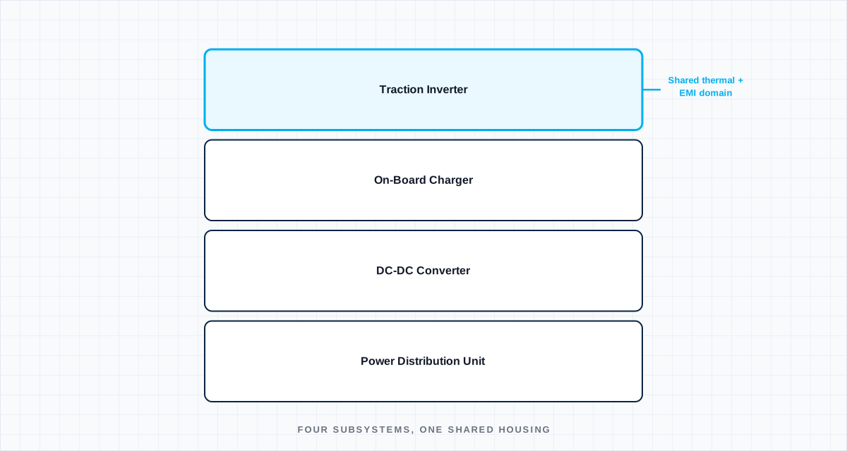
The commercial logic behind a 6-in-1 power electronics unit is straightforward: combine the traction inverter, on-board charger (OBC), DC-DC converter, and power distribution unit (PDU) — sometimes with additional functions like a secondary inverter for a rear motor — into a single housing, and you cut connector count, wiring harness mass, enclosure cost, and assembly time. The engineering logic is a lot less straightforward, because every one of those subsystems was originally designed to be its own thermally and electrically isolated box, and integration forces problems that simply don't exist whedesign-challenges.svg)
Thermal co-design: shared cold plate, different heat profiles
A traction inverter's power stage produces high, spiky thermal loads correlated with acceleration events — short bursts, high peak power. An OBC produces a lower, steadier thermal load over a much longer charging window. A DC-DC converter sits somewhere in between, with load tied to auxiliary system demand. Put all three on a shared cold plate and you no longer have three independent thermal design problems — you have one coupled problem where a charging event and a hard acceleration on the same trip can stack thermal load on the same coolant loop in ways that never show up if you only simulate each subsystem's worst case in isolation.
The failure mode that catches teams off guard: the traction inverter's SiC or IGBT power modules are usually designed with junction temperature margin sized against their own worst-case duty cycle. If the coolant inlet temperature is already elevated because the OBC was charging the pack ten minutes earlier and the cold plate hasn't fully recovered, that margin shrinks — and it shrinks in a scenario the inverter's own thermal model never saw, because that model was built assuming the inverter had the cold plate to itself. Coupled transient thermal simulation across all three subsystems' realistic duty cycles, not just each one's independent worst case, is the difference between a 6-in-1 unit that survives real-world drive-then-charge sequences and one that derates unexpectedly in the field.
EMI/EMC: proximity creates coupling paths that didn't exist before
Separate enclosures meant separate ground planes, separate shielding, and physical distance as a (crude but real) form of EMI mitigation. Inside a shared 6-in-1 housing, the traction inverter's high dv/dt switching edges — especially with SiC MOSFETs, where switching speeds are faster than legacy IGBT designs — are now physically centimeters from the OBC's control circuitry and the DC-DC converter's feedback loops.
Two coupling paths cause most of the pain in practice:
- Conducted common-mode noise through the shared DC bus, where the inverter's switching noise rides on the same bus rail the DC-DC converter is trying to regulate from, degrading output ripple on 12V/48V auxiliary rails in ways that are hard to trace back to the inverter because the two subsystems appear electrically independent on the schematic.
- Radiated coupling into low-level analog signals — current sensor outputs, temperature sensor lines, resolver signals — that were adequately shielded when routed meters away from a switching power stage, and are marginal when routed centimeters away inside a shared housing.
The fix isn't more shielding after the fact, it's zone-based layout planning from the start: partitioning the enclosure into high dv/dt zones and sensitive-signal zones with intentional physical separation and dedicated ground stitching, decided during mechanical layout, not discovered during EMC pre-compliance testing when the PCB is already routed.
High-voltage isolation on a shared PCB
When the traction inverter, OBC, and DC-DC converter each had their own board, each board's HV isolation strategy — creepage and clearance distances, isolation barrier placement — could be designed independently for that subsystem's voltage class. On a shared or closely-coupled PCBA, you're now routing multiple HV domains (main traction bus, charging-side HV, and low-voltage auxiliary) in proximity, and isolation design has to account for the worst-case voltage differential between any two domains that share board real estate, not just each domain's own rating.
This is where automotive PCB fabrication requirements — thick copper for current-carrying traces, controlled creepage/clearance per the relevant isolation standard, slotting or routing between HV and LV zones — stop being a per-subsystem decision and become a whole-board constraint that has to be locked before layout starts, because retrofitting isolation clearance into a routed board usually means a respin.
Functional safety: ASIL decomposition across shared hardware
When the traction inverter and the DC-DC converter (which may feed safety-relevant loads like brake system auxiliary power) lived in separate housings, their ASIL (Automotive Safety Integrity Level) decomposition was relatively clean — separate hardware, separate failure domains. In a 6-in-1 unit, a single shared power supply, a single shared microcontroller domain, or a single shared connector can become a common-cause failure point that couples safety domains that were supposed to be independent.
Getting this right means the functional safety concept has to be developed with the mechanical and electrical integration architecture, not layered on top of it afterward. If ASPICE process alignment work starts after the hardware architecture is frozen, safety decomposition ends up working around hardware decisions instead of informing them — and that's usually visible later as awkward, expensive mitigations (redundant sensing, additional isolation) that a slightly different partitioning decision earlier would have avoided entirely.
DFM/DFT for high-power automotive PCBA
None of the above matters if the board can't actually be manufactured and tested at automotive volume. High-power PCBA for a 6-in-1 unit typically means thick copper layers (2oz+ on power planes), thermal vias under power devices, and IPC-A-610 Class 3 workmanship standards for solder joints carrying real current under vibration and thermal cycling loads that consumer electronics never see.
Design-for-test matters just as much: a 6-in-1 board has far more test points and far more interacting subsystems to validate at end-of-line than three separate boards would, and test coverage planned late in the design cycle tends to miss internal nodes that become critical for field diagnostics later — meaning failures that are easy to see on the bench are hard to isolate on a returned unit two years into service, because the test points needed to isolate them were never brought out.
The underlying trade-off
A 6-in-1 unit is a genuine engineering win on cost, mass, and packaging — but every one of those wins is paid for with coupling: thermal coupling, EMI coupling, isolation coupling, and safety-domain coupling that a set of separate boxes never had to deal with. The projects that get through validation on schedule are the ones that treat that coupling as the primary design problem from day one, not as an integration issue to resolve after each subsystem is "done."
Define the boundary
Name the operating state, interfaces, tolerances and degraded conditions. A test without a boundary only proves the sample survived once.
Capture the right signal
Choose measurements fast and close enough to the mechanism to explain cause, sequence and margin—not just the final alarm.
Set a decision rule
Agree before the test what passes, what triggers redesign and what uncertainty requires another experiment.
Turn the lesson into a validation plan.
Bring us the requirement, failure signature or architecture boundary. We will help frame the evidence needed to make the next decision.