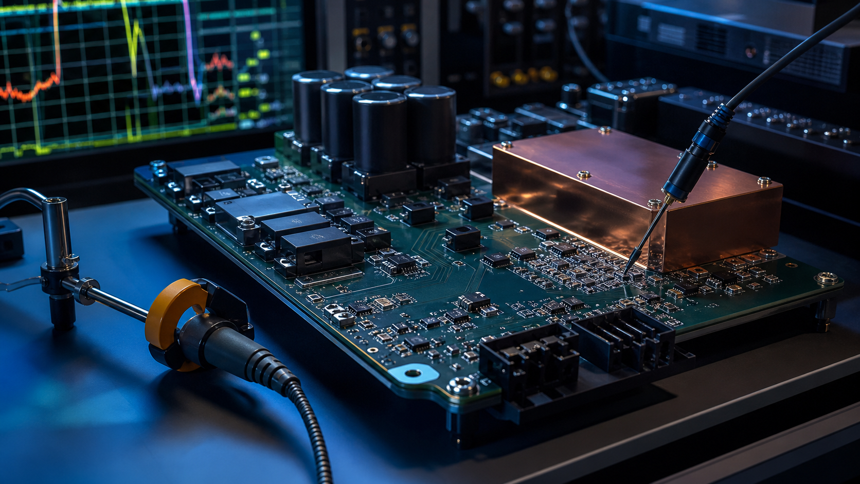
A schematic can be electrically correct while its PCB is an effective antenna. The gap comes from treating connections as ideal nets. At switching edges, current follows the path of lowest impedance, dominated by inductance and the nearest return plane—not necessarily the shortest resistance path drawn on the schematic. Every interruption, shared segment and large loop converts switching energy into voltage overshoot, common-mode current or radiation.
Identify the high di/dt and high dv/dt loops
In a half bridge, the critical commutation loop includes the DC-link capacitor and switching devices. Minimize its enclosed area and place high-frequency capacitance at the devices, not merely somewhere on the same net. The gate loop is separate and equally important: driver, gate resistor, device gate and Kelvin source or emitter return should form a compact controlled loop isolated from power-source inductance.
High dv/dt switching nodes should have minimal copper area consistent with thermal needs. Copper beneath them can increase parasitic capacitance into chassis or secondary circuits. Thermal spreading and EMI can therefore conflict; solve the thermal path deliberately rather than expanding the noisy node by default.
Return-path discontinuities create antennas
A signal crossing a split plane forces its return current to detour, enlarging the loop and coupling into other structures. Digital isolators and isolated power supplies do not eliminate common-mode current; their parasitic capacitance provides a high-frequency bridge. Place isolation components so primary and secondary return structures are controlled, and provide intentional common-mode paths only where the safety architecture permits them.
Connector pinout is part of layout. Put signal returns beside sensitive signals, terminate shields with low inductance at the enclosure boundary, and prevent noisy current from traversing the quiet-control region on its way to a mounting point or cable shield.
Component choice and placement are inseparable
A capacitor's useful impedance includes package, mounting and via inductance. A high-capacitance part placed far from the switching loop may contribute less at the edge frequency than a smaller, lower-inductance part at the device. The same principle applies to shunts, snubbers, common-mode chokes and TVS devices: layout parasitics are part of the component value.
Review package current paths, thermal pad connectivity, voltage coefficient, bias derating, pulse rating and failure mode. A part number is not qualified until its mounted behavior under real voltage, temperature and frequency is understood.
Pre-compliance as a design instrument
Use current probes, near-field probes, LISNs and controlled load states before formal EMC testing. Correlate spectral peaks with PWM carrier, edge ringing, clock families and control-state transitions. Change one mechanism at a time: gate resistance, snubber, shield bond or return path. A fix that lowers one peak but raises device loss or common-mode current elsewhere is a trade, not a solution.
Layout-review exit criteria
Close review when every fast-current loop can be traced physically, return paths remain continuous across layer transitions and connectors, isolation parasitics are intentional, filter components are placed relative to the noise boundary, and pre-compliance data covers worst-case voltage, load and switching mode. Passing a bench functional test provides almost no evidence for these conditions.
Define the boundary
Name the operating state, interfaces, tolerances and degraded conditions. A test without a boundary only proves the sample survived once.
Capture the right signal
Choose measurements fast and close enough to the mechanism to explain cause, sequence and margin—not just the final alarm.
Set a decision rule
Agree before the test what passes, what triggers redesign and what uncertainty requires another experiment.
Turn the lesson into a validation plan.
Bring us the requirement, failure signature or architecture boundary. We will help frame the evidence needed to make the next decision.